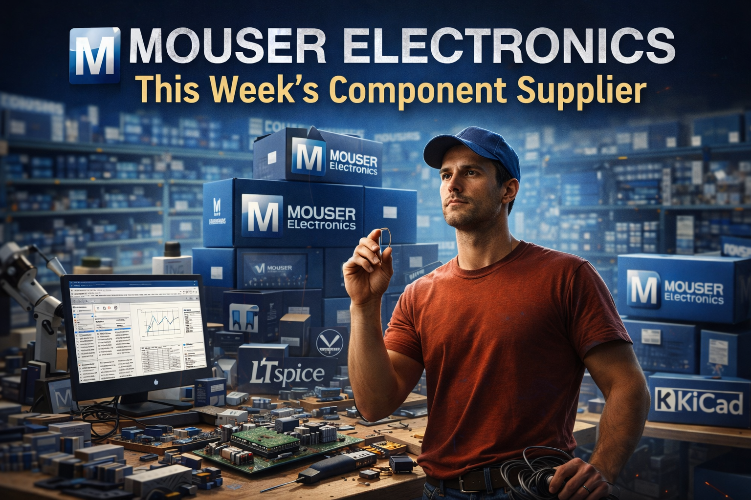
In any electronics project—especially one that lives somewhere between hobby and future product—the choice of component supplier quietly shapes everything that follows. Availability determines design flexibility. Documentation determines confidence. Packaging and models determine how fast an idea moves from schematic to board.
This week, I want to highlight Mouser Electronics as the primary component supplier I’m using for my current build, and explain why that choice matters at the bench level.
This isn’t a sponsorship. It’s a practical acknowledgment of how modern projects get built.
Selection That Enables Design (Not the Other Way Around)
One of Mouser’s strongest advantages is breadth—not just the number of parts, but the depth within each category. When you’re designing RF, analog, or mixed-signal circuitry, being able to compare multiple manufacturers’ parts side-by-side matters.
It means you can:
Adjust a design based on availability without starting over
Compare electrical characteristics, not just price
Avoid single-source dependencies early in a project
For small-scale builds, that flexibility is often the difference between continuing momentum and redesign fatigue.
Packaging Options That Respect the Builder
Not every project starts as a production run. Mouser’s packaging options—cut tape, reels, trays, and small quantities—support that reality.
That matters because:
Prototyping doesn’t require bulk commitments
You can validate a design before scaling
You’re not forced into unnecessary inventory cost early
It’s a small thing on paper, but at the bench it keeps experimentation affordable and sane.
Datasheets That Are Easy to Find—and Easy to Trust
Datasheets are not optional reading. They’re part of the design process.
Manufacturer datasheets (usually the latest revision)
Key electrical specifications at a glance
Environmental and compliance information
Lifecycle status (active, NRND, obsolete)
That saves time—and more importantly—reduces guesswork. When you’re validating operating limits or margin assumptions, having authoritative documentation one click away changes how confidently you design.
Parametric Search That Actually Works
Good parametric search isn’t about filters—it’s about decision-making.
This is especially useful when you’re designing under constraints imposed by cost, availability, or shipping considerations. It lets the design adapt to reality instead of fighting it.
Simulation and Footprint Models: Optional, but Powerful
While I’m currently using LTspice without vendor-specific component models, Mouser’s aggregation of simulation resources is worth noting.
SPICE or LTspice models (when provided by the manufacturer)
Manufacturer-supplied reference designs
In some cases, PCB footprint or pad layout data suitable for tools like KiCad
Even when you don’t use these models directly, their availability adds confidence. It means the component ecosystem around a part is mature, documented, and supported.
As the project evolves, those resources become increasingly valuable.
Why This Matters for Small Projects
Large organizations absorb sourcing friction through scale. Small builders don’t have that luxury.
A supplier that:
Presents clear specs
Supports small quantities
Aggregates documentation
Maintains predictable fulfillment
…becomes part of the engineering workflow itself.
That’s why Mouser fits well into this stage of my project. It supports exploration without forcing premature decisions about volume, vendor lock-in, or long-term commitments.
Final Thought
Choosing a component supplier isn’t about loyalty. It’s about alignment with how you build right now.
This project is still evolving. Designs will change. Constraints will shift. But having a supplier that reduces uncertainty—rather than adding to it—keeps the work moving forward.
Global trade wars are reshaping the economics of even small, personal projects. They aren’t stopping my work—but they are materially affecting how and when progress happens.
Comfort Zone — The Dream Phase (Technical Context)
I started this project the way many amateur radio builds begin: curiosity, excitement, and a notebook full of ideas. My attention was on problems I could reason about—oscillators, filters, frequency stability, PCB layout, and the satisfaction of turning schematics into something that actually emits RF. At that level, the challenge felt bounded, logical, and familiar.
What I wasn’t thinking about were tariffs, shipping lanes, trade policy, or geopolitics. For a long time, those factors stayed mostly invisible to individual builders. The global electronics supply chain, while complex, was optimized for efficiency: components were manufactured where it made economic sense, assembled elsewhere, and distributed through established logistics networks with relatively low friction for small orders.
By the time the broader trade environment shifted materially, I was already deep into the design.
Over the past several years, a combination of tariff changes, pandemic-era disruptions, fuel cost volatility, regional manufacturing realignment, and stress on global shipping routes has altered how electronic components move—and how costs are assigned. Policies enacted at the national level don’t just affect factories or large importers; they propagate through distributors, couriers, and pricing models until they surface at checkout, often in the form of minimum shipping charges or unexpectedly high delivery fees.
For large manufacturers, these costs can be negotiated, amortized, or absorbed through volume. For hobbyists and small buyers, they appear directly and disproportionately. I was operating without the scale, leverage, or insulation that larger organizations rely on.
At the outset of this project, though, none of that had yet intruded. The radio still existed only as a design concept. Parts were still just entries on a bill of materials. Suppliers felt interchangeable. The system appeared stable because most of its complexity remained hidden behind distributor websites and logistics abstractions.
At this stage, the problem still looked like an engineering problem—and engineering problems are, at least in principle, solvable.
Trigger — Reality Hits the Checkout Page
Then came checkout.
A small order from DigiKey—a handful of transistors, a couple of integrated circuits, and some basic resistors—suddenly carried a shipping quote north of $100. A separate order for five small PCBs fabricated overseas came back with nearly $40 in shipping, despite the boards themselves weighing almost nothing. In one case, tariff-related costs were embedded in courier fees, where a small shipment was consolidated into a larger customs-cleared order.
Nothing extravagant. Nothing exotic. No rush service. Just ordinary components moving through an extraordinary system.
It’s important to be clear here: this isn’t a criticism of any single company. Distributors, manufacturers, and logistics providers are operating within the same economic constraints as everyone else. Rising fuel costs, tariff structures, customs compliance, insurance, labor, and risk management don’t disappear simply because an order is small. These companies aren’t creating the pressure—they’re absorbing it and passing through what they can’t realistically carry themselves.
What becomes visible at this point is how fixed costs behave under stress. Brokerage fees, minimum courier charges, compliance overhead, and logistics risk premiums don’t scale down with order size. When those costs are spread across large volumes, they fade into the background. When they’re attached to a handful of components, they surface abruptly and without subtlety.
Large, well-capitalized organizations are structurally equipped to manage these pressures. They negotiate freight contracts, pre-position inventory, smooth volatility across volume, and treat logistics as a strategic function. Individual builders and early-stage projects don’t have access to those tools. Every order is effectively retail. Every shipment stands alone. Every inefficiency is fully exposed.
At this point, the project crossed an invisible boundary. The bill of materials stopped being just an engineering document and became a financial constraint. Design decisions were no longer driven solely by performance or elegance, but by shipping classes, country of origin, and minimum order economics.
This isn’t about fault. It’s about scale.
As someone who still intends to turn this work into a business after the small-scale prototyping phase, that distinction matters. Early experimentation lives in a narrow space between hobby and enterprise, but the current economic environment doesn’t treat that space gently. You’re not yet large enough to benefit from industrial efficiencies, but you’re already exposed to industrial pressures.
That’s the moment when the hobby stopped feeling like a hobby—and started feeling like a direct encounter with the realities of a stressed global system.
Crisis — In the Hole
This was the point where the work stopped.
Not because the engineering was beyond reach, but because the system surrounding it suddenly felt misaligned with small-scale effort. The rules hadn’t changed mid-project—but they had finally become visible.
I wasn’t out of ideas. I was out of confidence that the path forward made sense.
For the first time, continuing the build felt uncertain.
Recovery — Navigating the System, Not Fighting It
Climbing out of the hole didn’t happen by ignoring the system or pretending the pressure wasn’t real. It happened by learning how to navigate it more deliberately.
That meant rethinking how and where I sourced parts, how I staged orders, and how I treated procurement as part of the engineering process rather than a clerical afterthought. It also meant accepting that, at this stage, survival and momentum matter more than ideological purity.
One meaningful change came through PCBWay, who is sponsoring this project by helping offset PCB fabrication costs. That support doesn’t change the technical direction of the work, and it doesn’t come with editorial control or obligation. It simply improves the economics at the exact point where small-scale prototyping is most fragile.
It’s important to be clear about what this does—and does not—mean.
I am not a business yet. I am not operating as a brand. I am not beholden to any organization, distributor, or manufacturer. At this stage, the project remains independent, exploratory, and intentionally flexible. Sponsorship here is practical support, not alignment, endorsement, or exclusivity.
More broadly, recovery came from rejecting the idea that there is a single “correct” supplier or a moral hierarchy of parts. I’m navigating all available options—balancing cost, availability, quality, lead time, and risk in a system that no longer rewards simplicity. Every sourcing decision is contextual. Every choice is provisional.
This approach isn’t about cutting corners. It’s about keeping the project viable long enough to grow.
Because growth is still the goal.
I intend for this work to move beyond small-scale prototyping. When it does, the nature of these relationships will change. Real partnerships—mutual, explicit, and contractual—belong at that later stage. Who comes along for that ride will be determined by shared values, technical excellence, and clear agreements made on equal footing.
For now, recovery means staying in motion. Building carefully. Choosing pragmatically. And refusing to let structural pressure end the work before it has a chance to become something more.
A Better Place — Momentum, Perspective, and Optionality
The better place isn’t one where the system suddenly becomes fair or friction disappears. These pressures will continue. It’s a place where the constraints are understood, navigable, and no longer paralyzing.
What changed wasn’t the global economy—it was my posture within it.
By this point in the project, forward motion had returned. Not because costs dropped to zero or complexity vanished, but because enough paths opened up to keep building responsibly. That progress didn’t come from any single source. It came from a loose network of suppliers and service providers who, intentionally or not, make small-scale work like this possible.
Companies such as Mouser Electronics and Coilcraft provide access to high-quality components with transparent specifications and predictable fulfillment—critical when design margins are tight. PCBWay has helped materially by sponsoring PCB fabrication, easing the most fragile economic pressure point of early prototyping. Commodity sourcing through Amazon and Walmart fills gaps where precision is less critical but availability matters. Specialized vendors and logistics providers round out the ecosystem.
None of these companies dictate direction. None require loyalty. None are owed narrative control. What they provide—through services, access, or support—is optionality. And optionality is what keeps early-stage technical work alive.
This is the part of the process that often goes unnamed: building today requires not just technical skill, but supply-chain literacy. Knowing where flexibility exists, where costs hide, and where trade-offs are acceptable has become part of the craft. The workbench now extends into procurement decisions, logistics timing, and economic judgment.
That’s not a loss. It’s an adaptation.
I’m still not a business. I’m still not operating as a brand. But I am building with intent. I’m learning which relationships scale, which ones are situational, and which values I’ll want reflected when formal partnerships eventually make sense. When that time comes, the agreements will be explicit, mutual, and grounded in shared goals—not necessity.
For now, the better place is simple: the project is alive, the radio is still being built, and the path forward—while more complex than it once seemed—is visible again.
And that’s enough to keep going.
Why This Story Is Structured This Way
This article uses the “Man in a Hole” story structure—moving from stability, through disruption, into recovery and growth. I learned this framework from Steve Rawling, whose work on storytelling (including Pip Decks) has influenced how I think about communicating technical journeys.
Storytelling matters—even in engineering—because context helps others recognize their own experience in yours.
My About page provides the background of my project, the Freedom7 HF Transceiver.
If this story resonates, comments are welcome. You can also reach me at david [at] kr4bad-dot-communications. no com
And if you believe understanding matters more than black boxes, you can subscribe to my WordPress https://kr4bad.com/?subscribe=1.
Over the past year, from a desk in my home in Fuquay Varina, North Carolina, I’ve been building a high-performance HF SSB transceiver from scratch. This Freedom7 HF Transceiver project has been a great journey but I need collaborators. Here’s the reality.
One person. No team. No funding. No company.
In that time, I’ve designed multiple microcontroller systems, written embedded C++ code, completed two full versions of receiver-chain band-pass filters, implemented seven switched BPFs on the input side, built encoder-driven VFO control with selectable step sizes, and displayed live frequency data on a working front panel — and that’s just part of the story.
This is not theory. This is real hardware, real software, and real progress.
And I need help.
“I Could Never Do What You’re Doing”
When I share this project with friends in my radio club, the Johnston Amateur Radio Society (JARS), I often hear the same thing:
“I could never do what you’re doing.”
I want to say this clearly and respectfully:
That belief is wrong — and it’s holding something back.
Most people assume that helping with a project like this means you have to be an RF expert, a programmer, or a career engineer. That’s simply not true. World-class systems are not built by one skill set — they’re built by people with different strengths working toward the same goal.
Let Me Be Very Clear About What This Is (and What It Is Not)
I want to remove any uncertainty right up front.
The Freedom7 HF transceiver project will be an example of what can be achieved when we collaborate.
Exploring the Freedom7 HF Transceiver Project
I am not forming a business right now
I am not asking for money or investors
I am not asking anyone to quit their job
I am not making promises or selling anything
The Freedom7 HF transceiver is not just a personal project; it’s an opportunity for collaborators to see if we can collectively build something huge.
What I am looking for is interest.
Genuine interest from people who want to be part of something being built carefully, honestly, and correctly — one piece at a time.
The Freedom7 serves not only as a technical challenge but also as a platform for sharing knowledge.
Who I’m Looking For (Hint: My radio friends could be collaborators)
You do not need to be an RF engineer to contribute.
I’m interested in hearing from:
Joining the Freedom HF transceiver project means becoming part of a community that values innovation and craftsmanship.
Builders and solderers
Tinkerers who like assembling things
Testers who enjoy finding what doesn’t work
Documentation writers and editors
Software developers (any level)
Engineers from any discipline
People curious about U.S. manufacturing
Legal or regulatory minds
Organizers, planners, and strategists
Folks who just want to learn by doing
If you’ve ever thought:
Through the HF SSB transceiver, I hope to inspire others to pursue their engineering passions.
“I’d love to help build something real.”
Then this project might be for you.
I see this project as a way to engage with others who share a love for radio technology.
Why This Matters to Me
I spent 15 years helping build nuclear submarines for the U.S. Navy. We were doing world-class work then, and I still believe that kind of discipline, pride, and craftsmanship matters.
I also believe we’ve lost something along the way — not just manufacturing capability, but the habit of building things together.
This radio project is my attempt to reclaim a small piece of that.
Not with hype. Not with shortcuts. And not by rushing to market.
But by designing a radio the way world-class systems are built: modular, testable, documented, and understood.
Where This Might Go (and Why That’s Okay)
Maybe this becomes a kit someday. Maybe it turns into a small U.S. manufacturer. Maybe it remains an open learning project.
I don’t know yet — and that’s okay.
What I do know is this:
Every detail of the Freedom7 HF transceiver matters, and I appreciate all the help offered.
Understanding the Freedom7 HF transceiver will help us face challenges and innovate.
Good things are built one honest step at a time, and they’re built better together.
This project will be a testament to our dedication and teamwork.
That’s the standard I’m holding myself to.
My One-Sentence Philosophy (Use This Anywhere)
Here’s the line you asked for — your repeatable, plain-spoken anchor:
“I’m not trying to build a company — I’m trying to build something worth building.”
That’s the heart of this entire effort.
An Open Invitation
By focusing on the HF SSB transceiver, we will create something truly special.
If this resonates with you — even a little — I’d like to hear from you.
No resumes. No commitments. No obligations.
Just interest.
Because no meaningful system — radio or otherwise — is ever built alone.
You can also read about my goals and strategy here.
My About page provides the background of my project, the Freedom7 HF Transceiver.
If this story resonates, comments are welcome. You can also reach me at david [at] kr4bad-dot-communications. no com
And if you believe understanding matters more than black boxes, you can subscribe to my WordPress https://kr4bad.com/?subscribe=1.
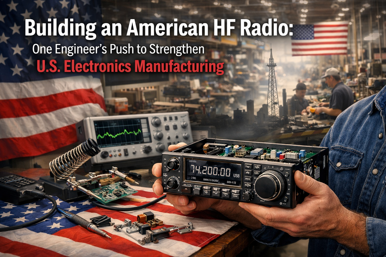
We could strengthen U.S. Electronics Manufacturing with evolution of a U.S.-built HF SSB Transceiver. The United States is pouring historic investment into semiconductor fabrication, and that’s essential for national capability. But the layers above the silicon—RF design, analog engineering, PCB layout, assembly, testing, and small‑batch manufacturing—are just as critical. They’re where ideas become devices, where engineers learn by doing, and where innovation doesn’t require a billion‑dollar cleanroom.
That’s the layer I’m stepping into with everything I’ve got.
I’m building an HF radio from scratch in the U.S., and I’m doing it with full transparency about the partners who make it possible. I’m not a giant corporation. I’m the new guy—the nascent partner in a re‑emerging American electronics ecosystem. But I’m pushing hard, and I can see the path forward.
🛠️ The early foundation: real partners, real parts
Every project starts with a supply chain, and mine is built on companies I trust:
Mouser for foundational components, authorized sourcing, and predictable quality
Coilcraft for inductors that behave exactly the way RF filters demand
Amazon for miscellaneous parts, tools, and materials—origin unknown, quality verified
PCBWay for fast, consistent PCB manufacturing during the prototyping phase
These aren’t anonymous vendors. They’re part of the story. They’re the reason my early boards exist, the reason my filters resonate where they should, and the reason I can iterate quickly.
🇺🇸 Why the U.S. needs more than fabs
Chip fabs are vital, but they’re not the whole picture. The U.S. also needs:
U.S. Electronics Manufacturing (small companies that can support markets at first)
Engineers who can design RF circuits
Technicians who can assemble boards
Small labs that can prototype quickly
Companies that can build specialized hardware in low to medium volumes
U.S. Electronics Manufacturing needs workplaces where Americans solve hands‑on technical problems
This is the layer where a single engineer can make a difference. This is where small companies grow into meaningful contributors. This is where I want to build something real.
📡 The HF radio as a proving ground
My HF radio project isn’t just a hobby. It’s a forcing function—a way to build capabilities that scale:
High‑Q inductors for 160 m and 10 m filters
Stable, low‑noise RF amplification
Clean, reproducible PCB layouts for multi‑band RF paths
Repeatable assembly processes
Documentation that others can follow
Every solved problem becomes a skill. Every skill becomes part of a future U.S. Electronics Manufacturing workflow.
This is how a one‑person lab becomes a small manufacturer.
🌱 The long‑term vision
I want to grow into a U.S. electronics design, assembly, and U.S. Electronics Manufacturing company that:
Builds RF hardware with care and transparency
Manufactures boards domestically whenever possible
Partners openly with global suppliers
Creates challenging technical jobs for Americans
Strengthens the layers of the electronics ecosystem that sit above the silicon
I’m not trying to compete with semiconductor fabs or big manufacturers. That’s not my lane, and it never has been.
What I’m building lives in the layer those fabs make possible — the part of the process where real innovation actually happens. It’s the space between raw silicon and a finished product, where radios are thought through, designed, tested, and built one hard decision at a time.
That’s where Freedom7, my HF transceiver project, lives. Not on a factory floor and not in a boardroom, but at a workbench — where schematics turn into boards, code meets copper, and performance is earned through testing and iteration.
This is the part of engineering you can’t rush, outsource, or fake. It’s where ideas either work or they don’t. And it’s the kind of work I know how to do, because it’s how I’ve always done things.
This is early. This is small. But it’s real. And I’m pushing hard because I can see what it could become. I’m excited about the influx of investment here and I see a bright future for U.S. Electronics Manufacturing maybe on a smaller scale than the AI chip fabs.
I’m a real person, find about me, my character, my personality, my integrity at Facebook.
My small order for a single PCB, required the manufacture of at least 5 PCBs of the same type. The boards were shipped with DHL direct to my home from PCBWay in China. Quality and value are what arrived in well-packaged box on my front porch.
Arrival
The boards arrived exactly as notified. I was impressed with the care taken in packaging—the box was well protected, and the PCBs were sealed in PCBWay’s packaging with desiccant included for moisture control. All five boards were clean, flat, and well protected.
I inspected the boards for any visible manufacturing defects and found none. The finished PCBs accurately reflected the Gerber and drill files I provided to PCBWay.
Inspection
This PCB design had pads I designed to provide a mounting for Harwin RFI enclosure clips. I realized during assembly that the surface tension at solder melt would perfectly align these clips. PCBWay oriented them 90 degrees to how they should have been, again exactly as I specified in the Gerber files. I measured these pad coordinates relative to the edge references and they were perfect! We’ll fix that final version.
I am constantly aware of the heat being applied to the SMD components. I was closely paying attention to the PCB as items were individually being soldered. I.e. I was looking for any defect in the printed circuit board (PCB) from the high temperature being used with the liquid solder (285 C). Everything held together for the entire assembly.
Because this design uses surface-mount components, I paid close attention to how the board handled heat during soldering. Each component was soldered individually at approximately 285 °C, and I carefully watched for any signs of delamination, pad lifting, or trace damage. The PCB remained mechanically and electrically sound throughout the entire assembly process.
The product was solid.
I did not individually probe every trace. For a large or densely populated board, I likely would have. This design is intentionally simple—three inductors and five capacitors forming an RF filter—so functional testing after assembly was the most practical and meaningful validation.
To complete the RF shielding, I fabricated a cover using 0.2 mm sheet aluminum. This enclosure, open on the bottom, mates with the Harwin clips and fully shields the passive RF components.
Testing
Final testing was performed using a NanoVNA. The results exceeded my expectations, with an insertion loss of just –0.84 dB. Yes—very pleased with that result.
Final Review
Overall, I was extremely satisfied with the entire PCB manufacturing experience, from the initial order process through final testing. Every stage—shipping updates, production notifications, delivery timing, arrival condition, physical inspection, verification against design files, hands-on assembly, and final RF performance testing—met or exceeded my expectations for a professionally manufactured printed circuit board.
I am not a salesperson or affiliate. I approach this strictly as a designer and engineer who cares deeply about accuracy, repeatability, and real-world performance. From that perspective, PCBWay delivered exactly what was promised. The finished boards matched my Gerber and drill files precisely, arrived well-packaged and protected, and withstood both mechanical handling and high-temperature soldering without issue.
What stood out most was the overall workmanship-to-price ratio. For a technically demanding RF project—specifically a 20-meter band-pass filter PCB—the manufacturing quality, dimensional accuracy, and electrical reliability were excellent, especially given the cost. The boards performed as designed once assembled, and the measured RF results confirmed that the PCB fabrication did not introduce unexpected losses or defects.
Based on this experience, I can confidently recommend PCBWay to other engineers, designers, and amateur radio builders who are looking for reliable PCB manufacturing services at a competitive price. The combination of order creation, build workmanship, general communication, shipping notifications, and product value makes PCBWay a strong choice for both prototype and small-batch production work.
I’ll also refer this posting mentioning PCBWay ‘s suite of other services.
My About page provides the background of my project, the Freedom7 HF Transceiver.
If this story resonates, comments are welcome. You can also reach me at david [at] kr4bad-dot-communications. no com
And if you believe understanding matters more than black boxes, you can subscribe to my WordPress https://kr4bad.com/?subscribe=1.
The NanoVNA has become one of the most popular handheld vector network analyzers among hobbyists, RF engineers, antenna builders, and experimenters. It’s compact, affordable, and surprisingly capable. But there’s one critical step that determines whether your measurements are meaningful or misleading:
Calibration
If you skip calibration—or perform it incorrectly—your NanoVNA will still display curves and numbers, but they won’t reflect the true behavior of your device under test. Before every measurement session, and especially whenever you change frequency ranges, cables, adapters, or test fixtures, you must calibrate the instrument.
This guide walks you through why calibration matters, when to do it, and how to perform a proper SOLT calibration (Short, Open, Load, Thru) on the NanoVNA.
Why Calibration Matters
A VNA doesn’t measure your antenna, filter, or cable directly. Instead, it measures the combination of:
the device under test
the test cables
the connectors
internal imperfections
frequency response of the instrument
stray capacitances and inductances
Calibration mathematically removes these unwanted influences so the NanoVNA can isolate the behavior of the device you actually care about.
Without calibration, you may see:
incorrect SWR
shifted resonance points
wrong impedance values
misleading return loss
distorted S‑parameter curves
Even a high‑end lab VNA requires calibration. The NanoVNA is no different.
When You Should Recalibrate
You should calibrate every time you:
change the frequency sweep range
swap cables or adapters
move the NanoVNA to a different environment
measure a different type of device (antenna vs. filter vs. cable)
haven’t calibrated in a while
A good rule of thumb:
If anything in the signal path changes, recalibrate.
What You Need
Your NanoVNA should come with a calibration kit containing:
Open standard
Short standard
50‑ohm Load
Thru (usually just a male‑to‑male or female‑to‑female adapter)
If you have upgraded to higher‑quality calibration standards, even better.
Step-by-Step: How to Calibrate the NanoVNA (SOLT Method)
The NanoVNA uses the industry‑standard SOLT calibration: Short, Open, Load, Thru.
Below is the full procedure.
1. Set Your Frequency Range First
Calibration is frequency‑dependent. Set your sweep range before calibrating.
Example:
Antenna work: 50–600 MHz
HF: 1–30 MHz
Filters: narrow ranges around the passband
On the NanoVNA:
Menu → Stimulus → Start / Stop
2. Connect Nothing to Port 1 (CH0)
This is your reference port.
3. Perform the OPEN Calibration
Attach the Open standard to Port 1.
On the NanoVNA:
Menu → Cal → Open
Wait for the sweep to complete.
4. Perform the SHORT Calibration
Remove the Open, attach the Short standard.
Menu → Cal → Short
5. Perform the LOAD Calibration
Attach the 50‑ohm Load.
Menu → Cal → Load
This step is crucial for accurate impedance and SWR readings.
6. Perform the THRU Calibration (for S21 / CH1)
If you plan to measure filters, cables, or transmission characteristics, you must calibrate the second port.
Connect Port 1 to Port 2 using the Thru adapter or a short coax jumper.
Menu → Cal → Thru
If you only measure antennas (S11), you can skip this step.
7. Save the Calibration
Once all steps are complete:
Menu → Cal → Save → Slot 0–4
You can store multiple calibrations for different frequency ranges.
8. Verify the Calibration
A quick sanity check:
Attach the 50‑ohm load
SWR should read very close to 1.0
Impedance should be near 50 + j0 Ω
If not, repeat the process.
Tips for Better Accuracy
Use high‑quality coax jumpers
Avoid touching connectors during calibration
Keep the calibration standards clean
Use torque‑controlled tightening if possible
Keep the NanoVNA stable during the sweep
Avoid cheap adapters that introduce reflections
Small details matter when you’re working at RF.
Why Calibration Before Measurement Is Non‑Negotiable
The NanoVNA is incredibly capable, but it is only as accurate as its calibration. A poorly calibrated VNA can easily mislead you into:
cutting an antenna to the wrong length
misdiagnosing a cable fault
misunderstanding a filter’s passband
thinking a device is mismatched when it isn’t
Calibration is not optional. It is the foundation of every meaningful measurement.
Final Thoughts
Calibrating the NanoVNA may feel like an extra step, but it’s the difference between guesswork and real RF insight. Once you build the habit, it becomes second nature—and your measurements will be dramatically more reliable.
If you don’t already have one … treat yourself to the NanoVNA .
I used mine to test my v2 20-meter band-pass filter here.
My About page provides the background of my project, the Freedom7 HF Transceiver.
If this story resonates, comments are welcome. You can also reach me at david [at] kr4bad-dot-communications. no com
And if you believe understanding matters more than black boxes, you can subscribe to my WordPress https://kr4bad.com/?subscribe=1.
AI is powerful — but it performs at its best when you give it context. That one word, context, is the difference between a vague answer and a useful one. I love analogies, so let me start with a story that perfectly illustrates how AI works, why it sometimes gets confused, and how a little backstory can completely change the outcome.
I have a lot of interests. My wife never knows what topic I’m going to jump into next. Add a splash of ADD and maybe a dab of autism, and you’ve got a recipe for delightful chaos. One minute I’m talking about antennas, the next minute I’m redesigning a circuit board, and somewhere in between I’m wondering where I left my digital calipers. Humor aside, this unpredictability is exactly what happens when people interact with AI without giving the backstory. When context is missing, the conversation feels scattered — and the results can be just as confusing.
Here’s the first thing I want folks to understand: AI is not Google. Search engines look for keywords; AI looks for understanding. Most people still type prompts like search queries, then wonder why the answer feels incomplete. The truth is simple — AI needs context to deliver meaningful, accurate, and helpful responses.
Sharing My Experience Via Context
I use AI every single day — for work, for hobbies, and for some very technical challenges. I’ve experimented with multiple AI platforms and models, and even when using highly capable systems, I’ve learned that they still need strong context. Sometimes the AI gets things wrong, but more often than not, it’s just doing the best it can with the context it was given. When I improve the context, the answers improve. It’s that straightforward.
Let me ground this in something real. I’m building a seven-band HF SSB transceiver — a HAM radio designed to communicate across the globe. My background is in electrical engineering with a heavy focus on digital systems and assembly language. Communications theory? We touched it, but building an entire HF transceiver from scratch is a different level of complexity. That’s where AI became my technical co-pilot.
At the beginning of this journey, my questions were broad. I’d ask something like, “How do I design a mixer stage?” and the answers were generic. Once I started adding backstory — my frequency range, my architecture, my available components, my goals for stability and cost — everything changed. The AI moved from giving textbook answers to giving practical guidance that matched my actual project. Same AI, different context, dramatically better results.
As a licensed HAM, I passed exams that covered electronics fundamentals, but not to the depth required to design an entire transceiver. AI has helped me bridge that gap by turning curiosity into structured learning. Sometimes it even answers questions I didn’t know how to ask — because the surrounding context helps it anticipate what I’m really trying to achieve. And when it makes a mistake? I challenge it. I provide more context. I say, “Nope, that doesn’t fit this design,” and suddenly the next answer aligns much closer with reality.
Think about it this way. If I ask my wife, “Honey, have you seen my digital calipers?” she might give me a blank stare because the context is missing. But if I say, “Honey, I’m trying to measure the distance between clips on my PCB so I can build an RFI enclosure — have you seen that silver measuring tool with the digital readout?” she instantly understands the context and points me to the dining room table… along with a reminder that it belongs in the garage. Same question, more background, completely different outcome.
That’s exactly how AI works. Context unlocks clarity. Context shapes relevance. Context reduces guesswork.
My goal here isn’t just to help you find your car keys or troubleshoot a circuit. My goal is to help you understand how to think when you interact with AI. The old saying still applies: “Garbage in, garbage out.” But today I’d rephrase it slightly — “Weak context in, weak results out.” When you give AI richer context, you’re not just asking a question; you’re building a shared understanding that leads to better collaboration.
Some people worry that AI will replace them. I don’t see it that way. AI is a tool — a very powerful hammer — but without context, every problem still looks like a nail. The real advantage belongs to the people who learn how to use context effectively. They’re the ones who get clearer answers, faster solutions, and deeper insights.
So here’s my elevator pitch: If you want better results from AI, don’t just ask questions — give context. Explain what you’re doing, why you’re doing it, what you’ve already tried, and where you’re stuck. Treat AI less like a search bar and more like a collaborator who needs backstory to help you succeed.
Because at the end of the day, you’re not going to be replaced by AI. You’re going to be replaced by someone who knows how to use AI with the right context — and knows how to swing that new hammer with confidence.
Try it. Use it. Tell it it’s wrong. My two favorites, Copilot and ChatGPT.
My About page provides the background of my project, the Freedom7 HF Transceiver.
If this story resonates, comments are welcome. You can also reach me at david [at] kr4bad-dot-communications. no com
And if you believe understanding matters more than black boxes, you can subscribe to my WordPress https://kr4bad.com/?subscribe=1.
A not-so-linear approach to creating a quality low noise amplifier for my HF transceiver.
I am very aware of AI, what it can do, how it works, and how it can let you down. I use it daily as an assistant as a professional IT architect. I took electrical engineering in college but my emphasis was digital logic and microprocessors. As an amateur radio operator, I have a great interest in how all these radios actually work. Some understanding is gained by study for the FCC license exams. I’m currently a General (second-level) operator. I am however, studying for my Extra (highest-level) license. This ticket allows more areas of the band spectrum that are off-limits to the lower-level licensees. Recently I’ve gained a lot of my detailed HF understanding using Microsoft Copilot’s AI during the design of components for my DIY HF transceiver the Freedom7.
I will take the reader through my design process here now and also share that I’ve already done this with failures. This is the not-so-linear aspect I referred to in my subtitle above. I’m currently working on a 20 meter band-pass filter for the second time. This post will describe my low noise amplifier (LNA) that comes after the band pass filters in the receive chain. The LNA is shown in the diagram below.
I have already designed switching mechanisms for 7 band-pass filters, for 10, 15, 17, 20, 40, 80, and 160 meters that are not shown in this diagram, but it shows the need for amplification after the passive band-pass filter to provide a serviceable signal at the mixer.
I designed this LNA already and I’ve even modeled it using LTSpice. I have a schematic in KiCAD but I left it and moved to LTSpice because I wasn’t satisfied with the design and wanted to model it’s behavior and understand it’s performance. Currently the best design that I have can be shared with the reader via the schematic in LTSpice.
To add to my not-so-linear wording in my subtitle, I’ll describe another failure (lesson-learned?) at this point in my design process here. I have a nice box with a wide range of ceramic capacitors and also electrolytics. I also have a cheap box of radial inductors with a wide selection of values. I modeled this on a breadboard. I think C3a should be an electrolytic (not shown). I broke out the 12v power supply, fired up the signal generator, and connected a 50 ohm connector to my oscilloscope. I expected beautiful results. Oh, how I was wrong!
With the help of Microsoft’s Copilot, I’m now going to explain this failure and the newfound education I’ve acquired.
When My 1–30 MHz LNA Met a Breadboard: A Cautionary Tale
Designing the LNA on paper felt elegant. Simulating it felt even better. Then I built it on a solderless breadboard — and everything fell apart. The amplifier oscillated, detuned itself, picked up every stray signal in the room, and generally behaved like it had a personal grudge against me.
So what happened? The short answer: breadboards and RF don’t mix. The long answer is much more interesting.
A solderless breadboard looks electrically simple, but at RF it’s a jungle of unintended components.
1. Breadboards Have Enormous Parasitics
Each tie point adds 2–5 pF of stray capacitance.
Each row has tens of picofarads between adjacent rails.
Every jumper wire adds tens of nanohenries of inductance.
At audio frequencies, these parasitics are irrelevant. At 1–30 MHz, they’re circuit‑destroying.
Your carefully tuned input network suddenly becomes a random LC filter. Your bias network becomes a resonator. Your transistor sees a completely different impedance than you designed for.
2. The Ground Plane Doesn’t Exist
RF circuits need a solid, low‑impedance ground plane. Breadboards offer the opposite:
Long, thin ground rails
High inductance
No shielding
No controlled return paths
The result? Your LNA’s ground reference floats, shifts, and radiates. The amplifier starts behaving like a tiny radio transmitter — and a very bad one.
3. Oscillation Becomes Almost Guaranteed
Wideband LNAs are inherently sensitive. They need:
Short leads
Tight layout
Controlled impedance
Proper decoupling
A breadboard gives you:
Long leads
Random layout
Undefined impedance
Decoupling capacitors connected through inductive rails
This is the perfect recipe for VHF oscillation, even if your design is only meant for HF. Many LNAs will happily oscillate at 80–200 MHz if you give them the chance — and a breadboard gives them every chance.
4. The Breadboard Acts Like an Antenna Farm
Every jumper wire is an antenna. Every row is a transmission line. Every gap is a slot radiator.
Your LNA ends up amplifying:
Local AM broadcast stations
Switching noise
Your laptop’s USB emissions
The fluorescent lights
The neighbor’s lawnmower ignition noise
Instead of a clean 1–30 MHz signal, you get a chaotic RF soup.
5. Power Supply Noise Goes Straight Into the Amplifier
Breadboards provide almost no isolation between:
Power rails
Signal rails
Ground returns
Even a clean bench supply becomes noisy once it hits the breadboard. Your LNA sees that noise as input signal and amplifies it gleefully.
The Takeaway
The LNA design wasn’t the problem — the construction method was. Breadboards are fantastic for digital logic, microcontrollers, and low‑frequency analog. But for RF, especially wideband RF, they’re essentially parasitic component generators.
If you want an LNA to behave, you need:
A copper‑clad ground plane
Short, direct connections
Proper shielding
SMD components if possible
A PCB or at least “Manhattan style” construction
My LNA didn’t fail because the design was bad — it failed because I built a precision RF amplifier on a device that’s basically a parasitic capacitor farm. Lesson learned: breadboards and megahertz don’t mix.
Decisions, Decisions: A Story to Explain
At this point in the LNA design process, do I proceed with the PCB manufacture? Do I add Harwin RFI shielding clip pads to the PCB? Am I really ready to pull the trigger on the PCB design using the schematic I’ll update in KiCAD from LTSpice?
My decision was to go through deep discussion with AI today and write this blog post, now describing my design of the LNA schematic in great detail. My post is aptly titled “Revolutionary New Design Process Includes AI” and while I want to re-validate my design, I’m going to provide the guidance I was originally given here in this post. This was more than just guidance, it was education. It really enlightened my understanding of the overall design process.
Designing a Low Noise Amplifier for HF: A Story to Sell Teamwork
I am certainly humbled by the power of AI and as a manager of people, I know the value of teamwork. I’m going to show the reader the value of using AI to answer all of the hard questions. At this point in time, my goal is to design an LNA for my HF radio that just works. My goal is described as follows:
Amplify very weak RF signals from the antenna with:
Low noise figure (NF)
Reasonable gain (10–20 dB is typical at HF)
Good input/output matching (usually 50 Ω)
Stability (no oscillations, no weird behavior with strong signals)
Linearity (doesn’t distort when a strong nearby signal appears)
At HF, the first active device largely sets the receiver’s noise performance. Everything I do in this stage—biasing, matching, layout—will feed into that.
My device has already been chosen. I have a supply of BFR93A SMD bipolar junction transistors on-hand. I think of this transistor as a transconductance device: input voltage → output current, then a load resistor/transformer turns that into voltage gain, hence the term amplifier. My LNA amplifies AC or RF signal input.
DC Bias
First and most importantly, I need to set the operating point of the transistor or amplifying device with DC bias. The transistor must sit at a quiescent point (Q‑point) where:
It’s in the region where noise performance is good
It’s in Class A (conducts over the full RF cycle)
It has enough headroom for signal swing
I would typically set:
Collector current : often 1–10 mA for HF LNA
Collector voltage : maybe half the supply (e.g., 6 V on a 12 V supply)
Base bias via a resistor divider or current source
Basic idea:
Choose for a good trade‑off between noise, gain, and power
Use a collector resistor such that:
Base bias network sets
Emitter Bypassing
In a Bipolar Junction Transistor (BJT) amplifier, the emitter resistor sets the transistor’s bias and stabilizes the gain. That resistor also introduces negative feedback, which keeps the amplifier linear and predictable, specifically needed for this sensitive amplifier.
But there’s a catch.
Negative feedback reduces gain — including the gain you want at RF.
Emitter bypassing is the technique of placing a capacitor in parallel with the emitter resistor so that:
DC still sees the resistor (for stable bias)
AC/RF sees the capacitor (which looks like a short at RF)
In other words:
The resistor controls the transistor at DC. The capacitor “turns off” the resistor at RF so you get more gain. See the balance here?
If you return to my schematic, I have 3 components here, R4, C3a, and C3b. My 10uF capacitor, C3a is electrolytic as a choice because it’s suited for the low frequency short.
Emitter bypassing is powerful, but it comes with trade‑offs. The emitter resistor provides negative feedback that helps prevent oscillation but by bypassing it, you remove that feedback at RF, reducing stability. This design choice affects all that bad stuff I talked about above. I’ll have the option of changing values on my PCB using SMD packaging when I’m at that point.
I’ll wrap up this section with my best explanation. In a low‑noise amplifier, the emitter resistor sets the transistor’s bias and keeps the circuit stable, but it also reduces gain and adds noise. By placing a capacitor across that resistor, we “bypass” it at RF frequencies. The transistor still sees the resistor at DC, so the bias stays stable, but at RF the capacitor looks like a short, restoring gain and improving the noise figure. The trade‑off is that bypassing removes some of the stabilizing feedback, so layout and grounding become more critical to prevent oscillation.
Input and Output AC Coupling
As RF is the signal we’re processing we need input and output AC coupling at both ends of the amplifier. We will use capacitors to handle this job. The input capacitor will block DC so that our biasing is unaffected. It will also pass our RF with proper reactance, really around 50 ohms at the lowest frequency of the amplifier’s bandwidth. I choose its value so its reactance at the lowest frequency of interest is small compared to 50 Ω:
For example, at 1.8 MHz, you might want , so in the hundreds of pF to a few nF. I think it’s currently 100nF and that’s subject to change. Again, notice the not-so-linear approach to all this.
The output coupling capacitor needs to do the same. Its value was chosen so its reactance is small at the lowest frequency of interest and it blocks DC from the collector/drain. It will pass RF to the next stage, the mixer.
Impedance Matching
Now we’re seriously going into uncharted territory. It’s also where this RF stuff seems like an art in itself. I want to start with the input matching. I want the source (antenna and passive filter, usually 50 Ω) to see a good match into the LNA input.
Input Match
But the transistor’s input impedance is not 50 Ω by default. It’s some complex value depending on:
Bias point
Device parameters (gm, β, capacitances)
Frequency
Realize at this point, we’ll interject a change between the true input and the transistor device. I would use a matching network:
L‑network (series L, shunt C or vice versa)
Transformer (turns ratio to transform 50 Ω to the desired impedance)
Tapped inductor or autotransformer
Band‑pass network (for selectivity + matching)
I’ll use an LC network because I already have a coupling capacitor that can partner in a series LC situation to give us the impedance close to 50 ohms.
Copilot AI helped me realize there’s no perfect solution here and this is yet another piece of the LNA puzzle that may need some trial and error component value changes. The impedance that gives minimum noise figure is often not the same as the impedance that gives maximum gain for the amplifier.
So one would choose a source impedance (via matching network) that:
Is close to the optimum noise impedance of the transistor at that frequency
Still gives enough gain and reasonable match
This is one of the core design tensions in an LNA. And, I need to get the datasheet and review my current schematic before I can give it final approval.
Output Match
In keeping with the broadband 1-30MHz concept, we can’t use any form of LC combo. And, as I’m writing this .. . I gave AI this prompt: “Now, I’m questioning a 100nF, 47uH LC series input matching combo.” It seems that my design for the AC coupling was satisfactory but the LC combo to get the impedance matching is off.
Not-so-linear is becoming my mantra. I have conveyed my methods and how I use AI to answer my questions and then I tailor more questions as AI educates me. And, I have found errors in my design at this point and I have not finished the full outline of the LNA design aspects.
Conclusions
I’m going to conclude the details here but I am going to share an outline of how this should go when the final design is solidified. If I write about “every aspect” of my HF LNA, a nice structure might be:
Measured vs. simulated performance (gain, NF, IP3, stability)
System role of the LNA in an HF receiver
Choosing the transistor and topology
DC bias design (with example calculations)
AC small‑signal model and gain derivation
Input and output matching (with Smith chart examples if you like)
Noise figure and how design choices affect it
Stability analysis and practical stabilization tricks
Power supply decoupling and RF chokes
Layout and construction details (lead length, shielding, grounding)
I tend to think that I will use this outline and write about each when my not-so-linear approach at this LNA is complete.
My About page provides the background of my project, the Freedom7 HF Transceiver.
If this story resonates, comments are welcome. You can also reach me at david [at] kr4bad-dot-communications. no com
And if you believe understanding matters more than black boxes, you can subscribe to my WordPress https://kr4bad.com/?subscribe=1.
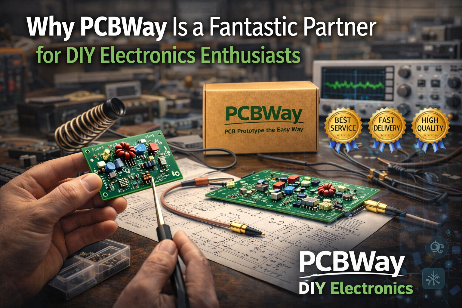
A personal look at their services, tools, and why I’m excited to collaborate with them. My current PCB supplier.
If you’re a home electronics tinkerer, maker, or radio hobbyist like me, you know the thrill of taking a design from idea to reality. Recently, I had the chance to work with PCBWay, and the experience has been so smooth, intuitive, and supportive that I felt compelled to share it.
What I discovered is that PCBWay isn’t just a PCB supplier. It’s a full ecosystem built with electronic engineers in mind.
A Maker‑Friendly Platform That Just Works
One of the first things that struck me was how intuitive and polished the PCBWay website is. Uploading my Gerber and drill files was effortless—the system immediately parsed the layers, confirmed the parameters, and guided me through the quoting process with clarity and zero friction.
For DIY builders, this matters. When you’re juggling CAD tools, schematics, and project deadlines, the last thing you want is a confusing ordering process. PCBWay gets this right.
Core Services Perfect for Hobbyists
1. PCB Supplier (Standard & Advanced)
PCBWay’s bread‑and‑butter service is their full‑feature custom PCB prototyping, available at low cost and with no minimum order quantity. Great for:
One‑off hobby projects
Rapid prototyping
Small‑batch builds
Learning PCB design without breaking the bank
They support everything from simple 2‑layer boards to advanced HDI, rigid‑flex, and multi‑layer stackups.
Here’s an example of a small two-layer board.
2. PCB Assembly (Optional but Powerful)
If you’re working with tiny SMD parts—or just want to save time—PCBWay offers affordable PCB assembly services. They handle:
Component sourcing
Soldering
Inspection
Testing (optional)
This is a huge win for hobbyists who don’t have reflow ovens or steady hands for 0402 components. I’m currently using 0805 but many aren’t doing SMD. PCBWay can help.
3. CNC Machining & 3D Printing
PCBWay has expanded far beyond PCBs. Their CNC machining and 3D printing services are ideal for:
Enclosures
Custom brackets
Knobs, gears, and mechanical parts
Prototyping housings for electronics
Their platform provides instant quotes and expert Design For Manufacturing (DFM) feedback, making it accessible even for beginners.
4. SMD Stencils
If you prefer assembling boards yourself, PCBWay offers precision SMD stencils—both framed and frameless. These are perfect for:
Hand‑soldering SMD components
Using solder paste with a hot plate or reflow oven
Improving assembly consistency
5. Online Tools for Makers
PCBWay includes a suite of free online utilities that are surprisingly useful:
Gerber Viewer
3D Viewer
Impedance Calculator
Trace Width Calculator
Electronic Design Viewer
These tools help you validate your design before ordering—something every hobbyist appreciates.
A Thriving Community for Inspiration
PCBWay hosts a massive project‑sharing community where makers post their builds, schematics, and tutorials. This is a goldmine for:
Learning new techniques
Finding inspiration
Sharing your own work
Connecting with other DIY enthusiasts
There are hundreds of beginner‑friendly projects, and new ones are added daily.
Why PCBWay Stands Out for Hobbyists
✔ No minimum order quantities
Perfect for one‑off builds and experiments.
✔ Fast turnaround times
Ideal when you’re iterating on a design or racing toward a project deadline.
✔ Excellent customer service
Many reviewers highlight PCBWay’s responsiveness and helpfulness—something I’ve experienced firsthand. There’s an online chat representative that helped me with my first order.
✔ Affordable pricing
Their low‑cost prototyping makes PCB design accessible to beginners and hobbyists.
✔ A true one‑stop shop
From PCB supplier to enclosures to assembly, they cover the entire workflow.
My Experience So Far
Uploading my PCB, Gerber, and drill files was seamless. The platform automatically checked the layers, flagged potential issues, and gave me a clear, transparent quote. The interface feels like it was designed by people who actually build electronics.
And the fact that PCBWay has been supportive of my radio project makes this collaboration even more meaningful. It’s refreshing to work with a company that values the maker community and actively supports hobbyists.
Final Thoughts
If you’re a DIY electronics enthusiast looking for a reliable, affordable, and hobbyist‑friendly manufacturing partner, PCBWay is absolutely worth your attention. Their combination of intuitive tools, broad service offerings, and community engagement makes them a standout choice for makers at any level.
I’m genuinely excited to continue working with them as my radio project evolves—and I hope this article helps other hobbyists discover what PCBWay has to offer.
I discussed their PCB quality in another post here.
My About page provides the background of my project, the Freedom7 HF Transceiver.
If this story resonates, comments are welcome. You can also reach me at david [at] kr4bad-dot-communications. no com
And if you believe understanding matters more than black boxes, you can subscribe to my WordPress https://kr4bad.com/?subscribe=1.
For years, surface‑mount devices (SMD) carried a reputation for being “too small,” “too fiddly,” or “only for factories.” Many Makers, HAM radio tinkerers, and DIY electronics hobbyists stuck with through‑hole parts because they felt safer and more familiar.
But the truth is this: with a little practice, a bit of flux, some liquid solder, and an inexpensive rework station, SMD work becomes not only approachable—it becomes fun. Once you learn the technique, you’ll wonder why you avoided it for so long.
This article is an invitation to give SMD a chance. You don’t need a professional lab. You don’t need a microscope. You don’t need a thousand‑dollar hot‑air station. You just need curiosity, a steady hand, and the willingness to try something new. I also use these glasses too. $20 on Amazon Yoctosun Magnifying Glasses with LED and headband
Why SMD Is Worth Learning
SMD components offer real advantages for home projects, especially as electronics continue to shrink and more parts become surface‑mount only.
1. SMD Saves Space—A Lot of It
Through‑hole components take up board area on both sides and require long traces to reach their pads. SMD parts sit flat on the board, allowing:
Smaller PCBs
Cleaner layouts
Shorter signal paths
More room for connectors, inductors, relays, and other bulky parts
In HF radio projects, this matters. You can reserve precious board space for the components that must be through‑hole—like toroids, high‑power RF transistors, or large electrolytic capacitors—while using SMD for everything else.
2. Many Modern Components Are SMD‑Only
If you want access to the latest ICs, filters, op‑amps, microcontrollers, and RF modules, SMD is often the only option. Learning SMD opens the door to:
Better performance parts
Lower noise amplifiers
Modern RF front‑end chips
Compact voltage regulators
High‑quality ceramic capacitors
You’re no longer limited to whatever through‑hole parts are left in the catalog.
3. SMD Can Actually Be Easier to Solder
This surprises people, but it’s true.
With through‑hole parts, you often fight with:
Leads that don’t fit
Pads that lift
Components that fall out while flipping the board
Excessive heat needed for large pins or ground planes
SMD, on the other hand, rewards technique over brute force. With flux and liquid solder, the surface tension does most of the work for you. Pads pull the solder into place. Components self‑align. Mistakes are easy to fix with hot air.
4. Rework Is Faster and Cleaner
A cheap hot‑air rework station can remove surface mounted ICs in seconds. Try doing that with a 40‑pin DIP without damaging the board.
For prototyping and experimenting, SMD is incredibly forgiving.
What You Actually Need to Get Started
You don’t need a professional setup. A beginner‑friendly bench can be built for less than the cost of a single high‑end soldering iron.
Here’s a realistic starter kit:
A basic hot‑air rework station (the inexpensive ones work fine)
A small‑tip soldering iron
Liquid solder (solder paste or low‑melt solder works great)
Good flux (this is the real secret weapon)
Tweezers
A magnifier or cheap USB microscope (optional but helpful)
Remember my glasses above
That’s it. No ovens, no fancy stencils, no industrial equipment.
Where Surface-Mount Fits in HF Radio Projects
HF radio designs often mix SMD and through‑hole parts. Not everything belongs has to be surface mounted, and that’s perfectly fine.
Great Candidates for SMD in HF Projects
Bypass and decoupling capacitors
Op‑amps and low‑noise amplifiers
Filters and matching networks
Microcontrollers and logic ICs
Voltage regulators
Small RF transistors
Resistors and small inductors
These parts benefit from short leads, low parasitics, and compact placement.
Better Left as Through‑Hole
Toroids and large inductors
High‑power RF finals
Large electrolytic capacitors
Connectors and mechanical components
Heat‑dissipating devices that need bolted heatsinks
Using SMD where it makes sense frees up board space for the components that must be larger or mechanically robust.
The Learning Curve Is Real—But Short
Your first few attempts may feel awkward. Components may fly off your tweezers. You might bridge a few pads. You might overheat a resistor or two.
But then something clicks.
You learn how much flux is “just right.” You learn how solder paste behaves under heat. You learn how to nudge a part into place and let surface tension finish the job.
And suddenly, SMD stops being scary and starts being empowering.
Why You Should Try SMD on Your Next Project
If you’re a Maker, a HAM, or a DIY electronics enthusiast, SMD opens up a world of possibilities:
Smaller, cleaner, more professional‑looking boards
Access to modern components
Faster assembly and rework
Better RF performance
More efficient use of PCB space
Most importantly, it expands what you can build at home.
SMD isn’t just for factories anymore. It’s for anyone with a soldering iron, a bit of patience, and the desire to push their skills forward.
Give it a try. You might discover that the “tiny parts” are not the enemy—they’re the gateway to better, more capable homebrew electronics.
My About page provides the background of my project, the Freedom7 HF Transceiver.
If this story resonates, comments are welcome. You can also reach me at david [at] kr4bad-dot-communications. no com
And if you believe understanding matters more than black boxes, you can subscribe to my WordPress https://kr4bad.com/?subscribe=1.