Category: Build Notes

How I think. What surprises me. What didn’t work. My intellectual edge and ego.

  • Why PCBWay is the Best PCB Supplier for DIY Electronics Enthusiasts

    Why PCBWay is the Best PCB Supplier for DIY Electronics Enthusiasts

    A personal look at their services, tools, and why I’m excited to collaborate with them. My current PCB supplier.

    If you’re a home electronics tinkerer, maker, or radio hobbyist like me, you know the thrill of taking a design from idea to reality. Recently, I had the chance to work with PCBWay, and the experience has been so smooth, intuitive, and supportive that I felt compelled to share it.

    What I discovered is that PCBWay isn’t just a PCB supplier. It’s a full ecosystem built with electronic engineers in mind.

    A Maker‑Friendly Platform That Just Works

    One of the first things that struck me was how intuitive and polished the PCBWay website is. Uploading my Gerber and drill files was effortless—the system immediately parsed the layers, confirmed the parameters, and guided me through the quoting process with clarity and zero friction.

    For DIY builders, this matters. When you’re juggling CAD tools, schematics, and project deadlines, the last thing you want is a confusing ordering process. PCBWay gets this right.

    Core Services Perfect for Hobbyists

    1. PCB Supplier (Standard & Advanced)

    PCBWay’s bread‑and‑butter service is their full‑feature custom PCB prototyping, available at low cost and with no minimum order quantity. Great for:

    • One‑off hobby projects
    • Rapid prototyping
    • Small‑batch builds
    • Learning PCB design without breaking the bank

    They support everything from simple 2‑layer boards to advanced HDI, rigid‑flex, and multi‑layer stackups.

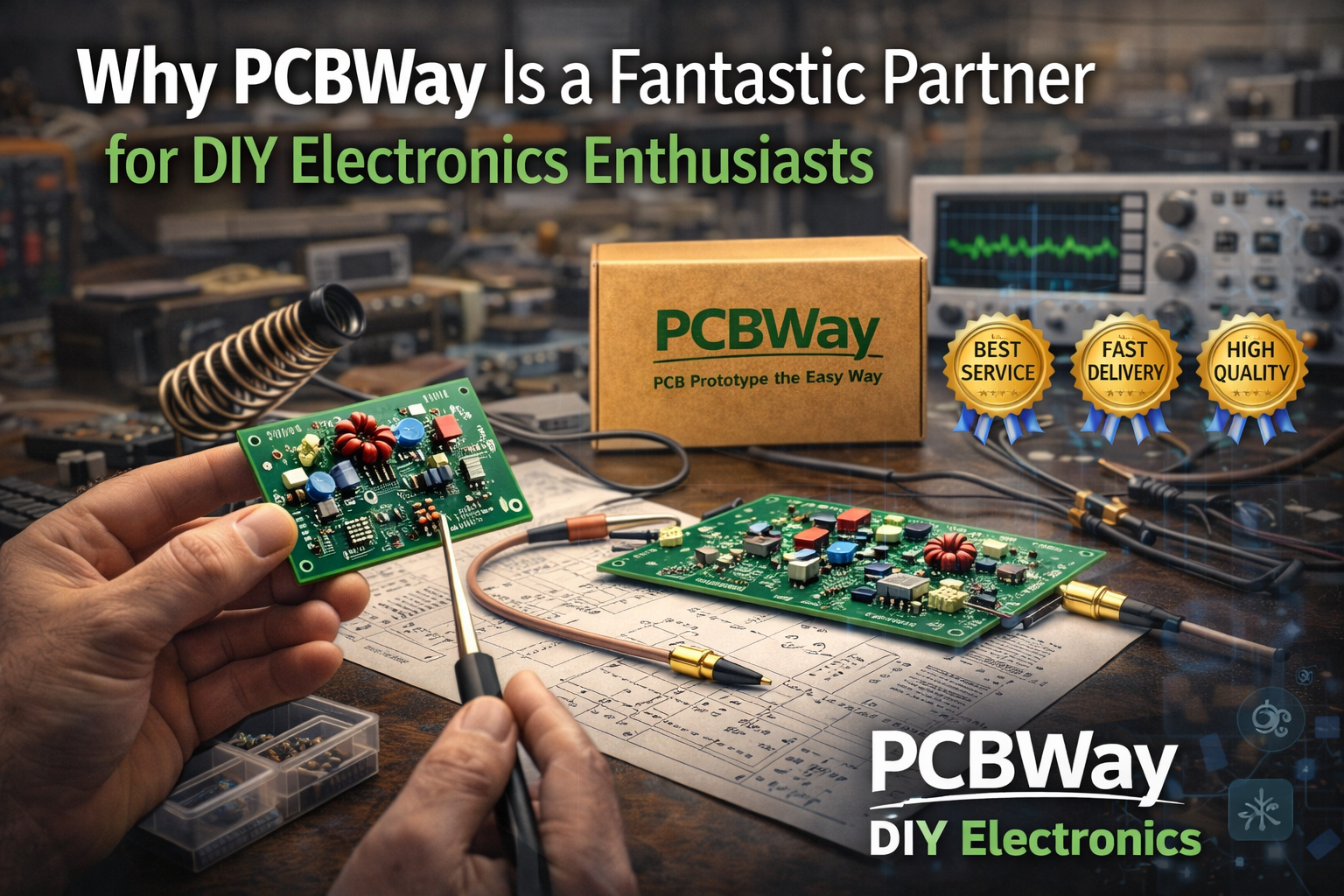
    Here’s an example of a small two-layer board.

    PCB supplier

    2. PCB Assembly (Optional but Powerful)

    If you’re working with tiny SMD parts—or just want to save time—PCBWay offers affordable PCB assembly services. They handle:

    • Component sourcing
    • Soldering
    • Inspection
    • Testing (optional)

    This is a huge win for hobbyists who don’t have reflow ovens or steady hands for 0402 components. I’m currently using 0805 but many aren’t doing SMD. PCBWay can help.

    3. CNC Machining & 3D Printing

    PCBWay has expanded far beyond PCBs. Their CNC machining and 3D printing services are ideal for:

    • Enclosures
    • Custom brackets
    • Knobs, gears, and mechanical parts
    • Prototyping housings for electronics

    Their platform provides instant quotes and expert Design For Manufacturing (DFM) feedback, making it accessible even for beginners.

    4. SMD Stencils

    If you prefer assembling boards yourself, PCBWay offers precision SMD stencils—both framed and frameless. These are perfect for:

    • Hand‑soldering SMD components
    • Using solder paste with a hot plate or reflow oven
    • Improving assembly consistency

    5. Online Tools for Makers

    PCBWay includes a suite of free online utilities that are surprisingly useful:

    • Gerber Viewer
    • 3D Viewer
    • Impedance Calculator
    • Trace Width Calculator
    • Electronic Design Viewer

    These tools help you validate your design before ordering—something every hobbyist appreciates.

    A Thriving Community for Inspiration

    PCBWay hosts a massive project‑sharing community where makers post their builds, schematics, and tutorials. This is a goldmine for:

    • Learning new techniques
    • Finding inspiration
    • Sharing your own work
    • Connecting with other DIY enthusiasts

    There are hundreds of beginner‑friendly projects, and new ones are added daily.

    Why PCBWay Stands Out for Hobbyists

    ✔ No minimum order quantities

    Perfect for one‑off builds and experiments.

    ✔ Fast turnaround times

    Ideal when you’re iterating on a design or racing toward a project deadline.

    ✔ Excellent customer service

    Many reviewers highlight PCBWay’s responsiveness and helpfulness—something I’ve experienced firsthand. There’s an online chat representative that helped me with my first order.

    ✔ Affordable pricing

    Their low‑cost prototyping makes PCB design accessible to beginners and hobbyists.

    ✔ A true one‑stop shop

    From PCB supplier to enclosures to assembly, they cover the entire workflow.

    My Experience So Far

    Uploading my PCB, Gerber, and drill files was seamless. The platform automatically checked the layers, flagged potential issues, and gave me a clear, transparent quote. The interface feels like it was designed by people who actually build electronics.

    And the fact that PCBWay has been supportive of my radio project makes this collaboration even more meaningful. It’s refreshing to work with a company that values the maker community and actively supports hobbyists.

    Final Thoughts

    If you’re a DIY electronics enthusiast looking for a reliable, affordable, and hobbyist‑friendly manufacturing partner, PCBWay is absolutely worth your attention. Their combination of intuitive tools, broad service offerings, and community engagement makes them a standout choice for makers at any level.

    I’m genuinely excited to continue working with them as my radio project evolves—and I hope this article helps other hobbyists discover what PCBWay has to offer.

    I discussed their PCB quality in another post here.


    My About page provides the background of my project, the Freedom7 HF Transceiver.

    If this story resonates, comments are welcome. You can also reach me at david [at] kr4bad-dot-communications. no com

    And if you believe understanding matters more than black boxes, you can subscribe to my WordPress https://kr4bad.com/?subscribe=1.

    73 KR4BAD David

  • SMD: Why Every DIY Electronics Enthusiast Should Give Them a Try

    SMD: Why Every DIY Electronics Enthusiast Should Give Them a Try

    For years, surface‑mount devices (SMD) carried a reputation for being “too small,” “too fiddly,” or “only for factories.” Many Makers, HAM radio tinkerers, and DIY electronics hobbyists stuck with through‑hole parts because they felt safer and more familiar.

    But the truth is this: with a little practice, a bit of flux, some liquid solder, and an inexpensive rework station, SMD work becomes not only approachable—it becomes fun. Once you learn the technique, you’ll wonder why you avoided it for so long.

    This article is an invitation to give SMD a chance. You don’t need a professional lab. You don’t need a microscope. You don’t need a thousand‑dollar hot‑air station. You just need curiosity, a steady hand, and the willingness to try something new. I also use these glasses too. $20 on Amazon Yoctosun Magnifying Glasses with LED and headband

    Why SMD Is Worth Learning

    SMD components offer real advantages for home projects, especially as electronics continue to shrink and more parts become surface‑mount only.

    1. SMD Saves Space—A Lot of It

    Through‑hole components take up board area on both sides and require long traces to reach their pads. SMD parts sit flat on the board, allowing:

    • Smaller PCBs
    • Cleaner layouts
    • Shorter signal paths
    • More room for connectors, inductors, relays, and other bulky parts

    In HF radio projects, this matters. You can reserve precious board space for the components that must be through‑hole—like toroids, high‑power RF transistors, or large electrolytic capacitors—while using SMD for everything else.

    2. Many Modern Components Are SMD‑Only

    If you want access to the latest ICs, filters, op‑amps, microcontrollers, and RF modules, SMD is often the only option. Learning SMD opens the door to:

    • Better performance parts
    • Lower noise amplifiers
    • Modern RF front‑end chips
    • Compact voltage regulators
    • High‑quality ceramic capacitors

    You’re no longer limited to whatever through‑hole parts are left in the catalog.

    3. SMD Can Actually Be Easier to Solder

    This surprises people, but it’s true.

    With through‑hole parts, you often fight with:

    • Leads that don’t fit
    • Pads that lift
    • Components that fall out while flipping the board
    • Excessive heat needed for large pins or ground planes

    SMD, on the other hand, rewards technique over brute force. With flux and liquid solder, the surface tension does most of the work for you. Pads pull the solder into place. Components self‑align. Mistakes are easy to fix with hot air.

    4. Rework Is Faster and Cleaner

    A cheap hot‑air rework station can remove surface mounted ICs in seconds. Try doing that with a 40‑pin DIP without damaging the board.

    For prototyping and experimenting, SMD is incredibly forgiving.

    SMD

    What You Actually Need to Get Started

    You don’t need a professional setup. A beginner‑friendly bench can be built for less than the cost of a single high‑end soldering iron.

    Here’s a realistic starter kit:

    • A basic hot‑air rework station (the inexpensive ones work fine)
    • A small‑tip soldering iron
    • Liquid solder (solder paste or low‑melt solder works great)
    • Good flux (this is the real secret weapon)
    • Tweezers
    • A magnifier or cheap USB microscope (optional but helpful)
    • Remember my glasses above

    That’s it. No ovens, no fancy stencils, no industrial equipment.

    Where Surface-Mount Fits in HF Radio Projects

    HF radio designs often mix SMD and through‑hole parts. Not everything belongs has to be surface mounted, and that’s perfectly fine.

    Great Candidates for SMD in HF Projects

    • Bypass and decoupling capacitors
    • Op‑amps and low‑noise amplifiers
    • Filters and matching networks
    • Microcontrollers and logic ICs
    • Voltage regulators
    • Small RF transistors
    • Resistors and small inductors

    These parts benefit from short leads, low parasitics, and compact placement.

    Better Left as Through‑Hole

    • Toroids and large inductors
    • High‑power RF finals
    • Large electrolytic capacitors
    • Connectors and mechanical components
    • Heat‑dissipating devices that need bolted heatsinks

    Using SMD where it makes sense frees up board space for the components that must be larger or mechanically robust.

    The Learning Curve Is Real—But Short

    Your first few attempts may feel awkward. Components may fly off your tweezers. You might bridge a few pads. You might overheat a resistor or two.

    But then something clicks.

    You learn how much flux is “just right.” You learn how solder paste behaves under heat. You learn how to nudge a part into place and let surface tension finish the job.

    And suddenly, SMD stops being scary and starts being empowering.

    Why You Should Try SMD on Your Next Project

    If you’re a Maker, a HAM, or a DIY electronics enthusiast, SMD opens up a world of possibilities:

    • Smaller, cleaner, more professional‑looking boards
    • Access to modern components
    • Faster assembly and rework
    • Better RF performance
    • More efficient use of PCB space

    Most importantly, it expands what you can build at home.

    SMD isn’t just for factories anymore. It’s for anyone with a soldering iron, a bit of patience, and the desire to push their skills forward.

    Give it a try. You might discover that the “tiny parts” are not the enemy—they’re the gateway to better, more capable homebrew electronics.


    My About page provides the background of my project, the Freedom7 HF Transceiver.

    If this story resonates, comments are welcome. You can also reach me at david [at] kr4bad-dot-communications. no com

    And if you believe understanding matters more than black boxes, you can subscribe to my WordPress https://kr4bad.com/?subscribe=1.

    73 KR4BAD David

  • Testing

    Testing

    This builder supports fast failure. Read on … you’ll understand. Or, build on and you’ll understand too.

    The first modular component I designed and created was the PCB for seven unique band-pass filters. They are passive and I could use a NanoVNA to actually show the performance curve with the RF spectrum from the NanoVNA device. I have created the front-switching component for these band-pass filters and also a RX/TX switching component. There are many things to test. This post will consider the tools I currently have and the methods I will use with these tools.

    I have an inexpensive, but serviceable oscilloscope and a pretty decent smart multimeter. The multimeter can check capacitors, diode forward-voltage, and even temperature. I have breadboards and various power supplies with sufficient amperage needed. I try to prototype and test each unique network task, chip, configuration, digital logic, etc before PCB manufacture. I have LTSpice for circuit modeling. I used LTSpice heavily during my bandpass filter design. I did not model the RX/TX switching schematic.

    My first test of the RX/TX switching component was to power it on with 5V and adjust a potentiometer for my 28V biasing (block) against schottky diodes. I powered the module and a small inductor started smoking. Hard stop! I had to completely rethink my design and testing. I should have considered everything prior to making the PCB and choosing components. This was all prior to any real testing.

    My lesson learned here is to consider amperage in all cases. And while I’m very excited with these SMD components, again I need to pay attention to voltage, amperage, wattage, etc. or component rating basically. My RX/TX switching component is pretty solid design on the receive side because the RF power is nothing really. The transmitting side completely forgot the RF power it would see. I really need an interface between the transmitting side and the central antenna connector.

    I also learned that I need a signal generator. I need a unique fixed RF frequency to send through components. I have a NanoVNA and I’ve been told that it can emit fixed frequencies. I will learn about the NanoVNA or I will make a testing signal generator using the Si5351a that I will use for my VFO.

    I’m trying to make ultimate use of the tools that I have. This radio project has been expensive. I need to use my head for something besides a hat-rack like my Dad always said. I think I have what I need to get me through most of what I need to test but that means, more focus on design. I also need to write down my tests regardless of simplicity.

    In conclusion, I’ve determined that more effort is needed before schematic, component, and PCB acceptance. Every circuit that isn’t completely clear in my mind should be modeled if possible in LTSpice. And, the component BOMs should be scrutinized for ratings, specs, etc. beyond just PCB footprint. More of everything needs to be written down.

    “Support fast failures” … Tom Peters


    My About page provides the background of my project, the Freedom7 HF Transceiver.

    If this story resonates, comments are welcome. You can also reach me at david [at] kr4bad-dot-communications. no com

    And if you believe understanding matters more than black boxes, you can subscribe to my WordPress https://kr4bad.com/?subscribe=1.

    73 KR4BAD David